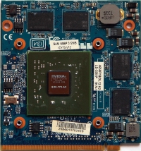
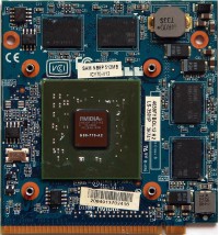
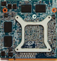
Mainstream mobile card based on G86 core (GF8400/8500).
Most cards, if not all, using DDR2 memory clocked only at 800-900MHz, compared to NVIDIA official clock 1400MHz using DDR3.
Vlask's card:
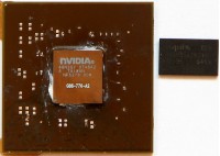
Chip is from Asus Z96S, MXM module is from Acer Aspire 5520G/7520G - 512MB DDR2.
Additional Info
- Made by: NVIDIA
- Codename: G86
- Bus: PCI-E x16, MXM, Integrated
- Memory Size: 512MB
- Max Memory Size: 512MB
- Memory Type: DDR2
- Year: 2007
- Announce Date: Wednesday, 09 May 2007
- Card Type: VGA
- Family: GeForce 8&9
- Manufacturer: TSMC
- Process tech: 80nm
- Transistors (Millions): 210
- Made in: Taiwan
- Owned by: Vlask (chip/not working)
- Outputs: 15 pin D‐sub
- Video Acceleration: MPEG-4 AVC (H.264)
- DirectX: DX10
- OpenGL: 3.3
- Core Clock (MHz): 600
- Shader Clock (MHz): 1200
- Effective Memory Clock (MHz): 1400
- Memory Bus Width: 128bit
- Memory Bandwidth (MB/s): 22400
- Texture Units: 8
- ROPs: 4
- Unified Shaders: 16
- Shader Model: 4.0 (DX10)
- Pixel Fillrate (MPixel/s): 2400
- Texel Fillrate (MTexel/s): 4800
- Sold by: AsusAcer
- Max Memory Clock (MHz): 1400
- Min Memory Clock (MHz): 800
- Press info: NVIDIA
- Wikipedia: Wiki
- Info: NVIDIA
- Info: Techpowerup
- Info: notebookcheck
Published in
NVIDIA Corporation


